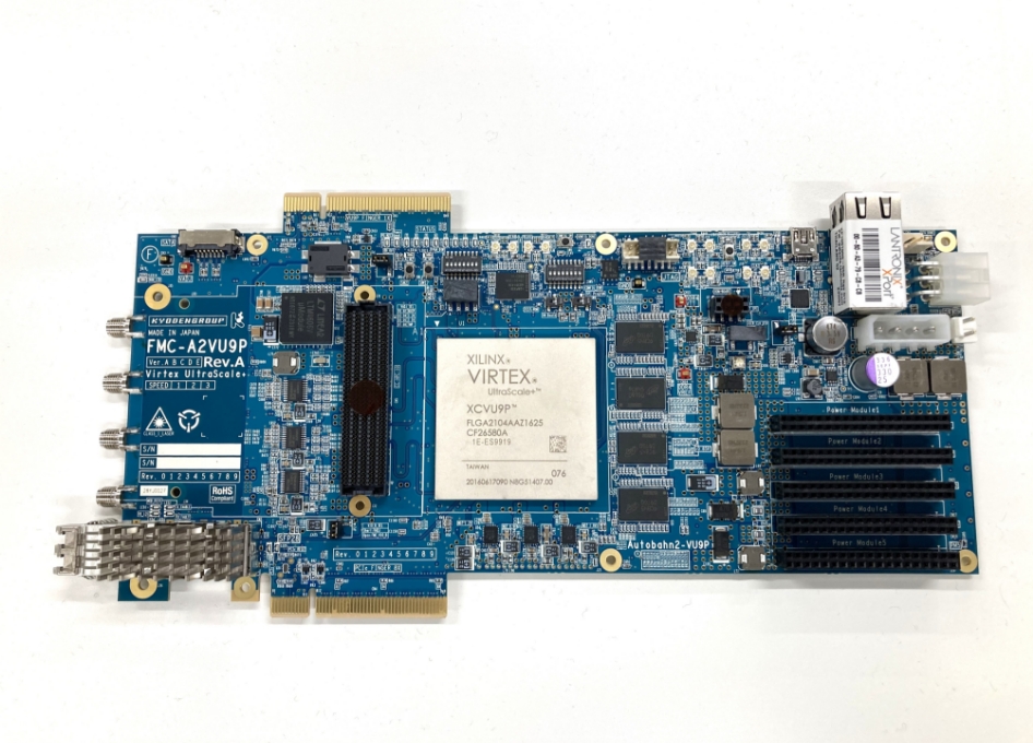
High-speed transmission PCBs
High-speed transmission PCBs are used to achieve high-speed data communication and high-speed signal transmission.
In order to achieve high-speed transmission, it is important to reduce transmission loss and reflection, and it is necessary to use low-loss materials and design PCBs that support high-speed transmission (signal line width, impedance, stub, etc.).
Features
- Used in applications such as high-speed communication network equipment and data center equipment.
- The data transmission speed is extremely high, and the latest communication technology is supported. This enables rapid transfer of large volumes of data.
- The impact signal attenuation and noise can be minimized. This improves signal quality.
- By using low dielectric constant, low dielectric loss materials, the transmission characteristics of signals are optimized, achieving performance suitable for high-speed communication.
KYODEN’s Strengths
- We can support hybrid configurations (low-loss materials + general materials).
- We have experience in everything from all-low-dielectric/low-loss substrates to hybrid structures.
- We have manufacturing know-how for high-frequency signal processing and reducing interference and noise.
- We can assist you from product development and propose layer structures including substrates and via structures.
- We have network analyzers. And we can also support Gbps-band simulations at KYODEN.
- We have experience manufacturing with fluorine substrates.
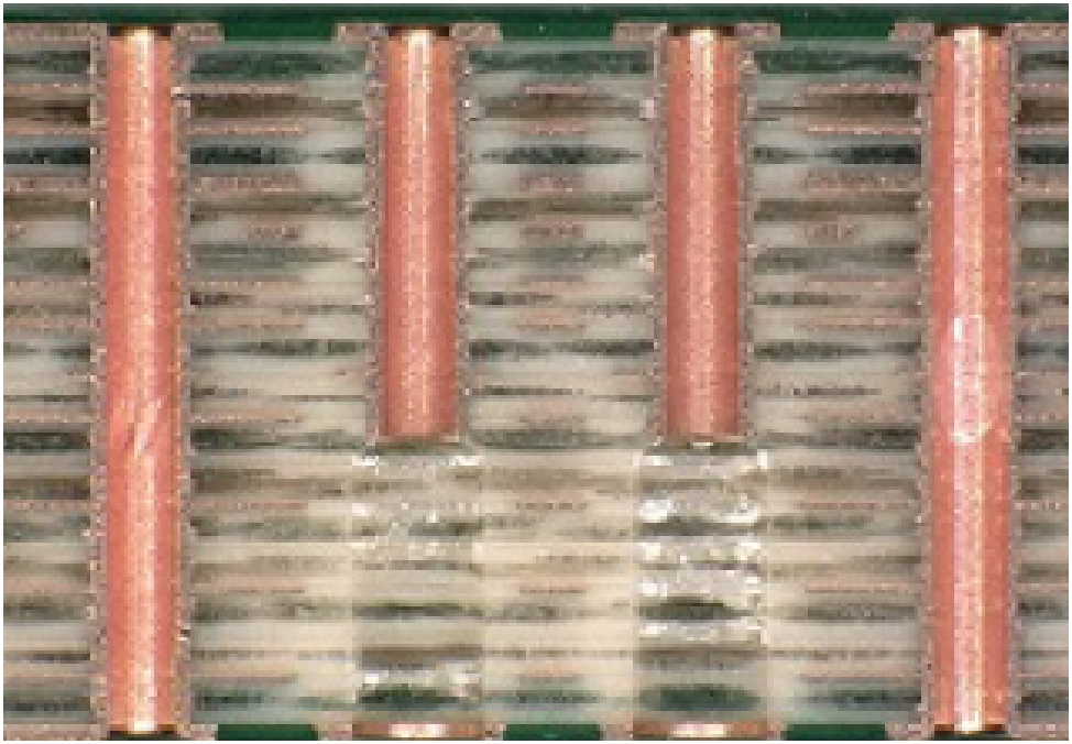
Back-drilled multilayer PCBs
Through-holes in transmission lines are a factor that reduces signal quality in proportion to the frequency, and by removing the excess portion of the through-hole (stub), it is possible to reduce signal reflection and improve transmission line characteristics.
Main product uses
- High-speed communication network equipment
- Data center equipment

