High heat-dissipating PCBs(high-speed heavy copper plating)
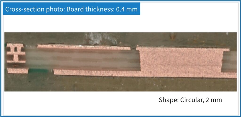
The area directly below the heat-dissipating components is filled with high-speed thick copper plating, and heat is dissipated by connecting directly to the bottom of the PCB with copper, which has high thermal conductivity.
Because it is formed using copper plating, it is easier to adapt to irregular shapes than with other methods (such as copper inlay), and it can be used on thin boards, which is difficult to do with copper inlay or copper coin.
Features
- Support for thin boards (t0.60 mm or less).
- Flexible support for irregular shapes.
- Connected by a heat dissipation surface (copper foil) and copper plating.
- Excellent heat dissipation characteristics without losing high-frequency characteristics.
- Reduces component degradation by improving heat dissipation characteristics, and also reduces transmission loss by shortening the wiring distance (wiring length).
Development product
PCB cross-section diagram
HDI Any Layer structure
Main product uses
- Power semiconductors
- High heat dissipation, high frequency components
- High-brightness LEDs, etc.

