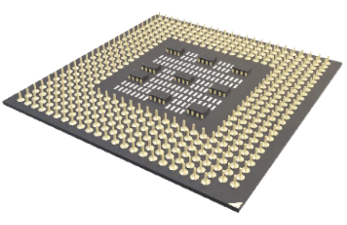
PCB design layout
Based on our extensive track record, we provide optimal component layout and cost proposals from a manufacturing perspective, as well as solutions to customer issues and concerns
KYODEN leverages its handles 5,000 PCB design projects a year. We can handle all types of PCB ranging from single-sided to multilayer types, as well as IVH, buildup, and flexible PCBs.
Moreover, because our services are not biased towards any particular sector, we handle a wide range of fields including automotive, medical, and industrial machines. Our team of 100 designers with Printed Circuit Board Manufacturing Technician, Level 1 or Level 2 qualifications realize artwork design with short lead time in consideration of mass production efficiency.
We can make proposals based on assessment data available precisely because we are a manufacturer.
PCB design layout
List of CAD software
| Category | Tool name | Manufacturer |
|---|---|---|
| PCB design layout | CR-8000 Design Force | Zuken |
| CR-8000 Board Designer | Zuken | |
| Allegro PCB Designer | Cadence | |
| OrCAD PCB Designer | Cadence | |
| Xpedition Layout | SIEMENS | |
| PADS | SIEMENS | |
| Manufacturing verification | Valor NPI | SIEMENS |
| DFM Center ADM | Zuken | |
| Viewer conversion | XDF Interchanger | Zuken |
| NDB Writer | Sohwa&Sophia Technologies |
We can also handle products in all sorts of fields
-

Aviation / Aerospace / Defense
-

Social Infrastructure / Energy
-

Medical / Healthcare
-

Machines / Robotics
-

Measurement / Control
-

AV / Broadcasting Devices
-

Automobiles / Transport Machines
-

Automatic and Service Devices
-

Servers, PCs / Peripheral Devices
-

Wired and Wireless Communication Devices
-

Disaster Prevention / Security
-

Household Electrical Appliances
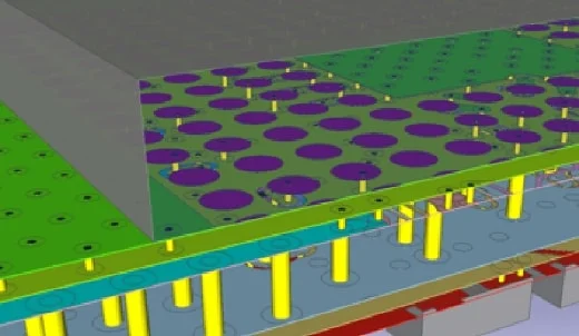
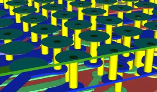
Leave High-density interconnect (“HDI”) design to KYODEN too
As the pitch of devices becomes increasingly narrow, many customers are faced with wiring difficulties.
In BGA/CSP packages, many of which increasingly have pitch of less than 0.4 mm recently, wiring is difficult in through-hole PCBs.
Because KYODEN manufactures High-density interconnect (“HDI”), we have abundant experience in designing such PCBs.
Laser via holes (LVH) used in High-density interconnect (“HDI”) have smaller diameters than drilled holes and are non-penetrating (penetrating only one layer), so they enable higher density mounting and more compact board sizes than through-hole boards and IVH PCBs.
They are also suitable for high-speed signal transmission, as via stubs can be avoided.
PTH PCBs

High-density interconnect (“HDI”)

Simulation
In development of electronic devices, one of the objectives of simulation is to “visualize things that are invisible to the eye.”
Full-time engineers, who also have experience of PCB design, leverage various types of simulation to provide high-quality PCBs.
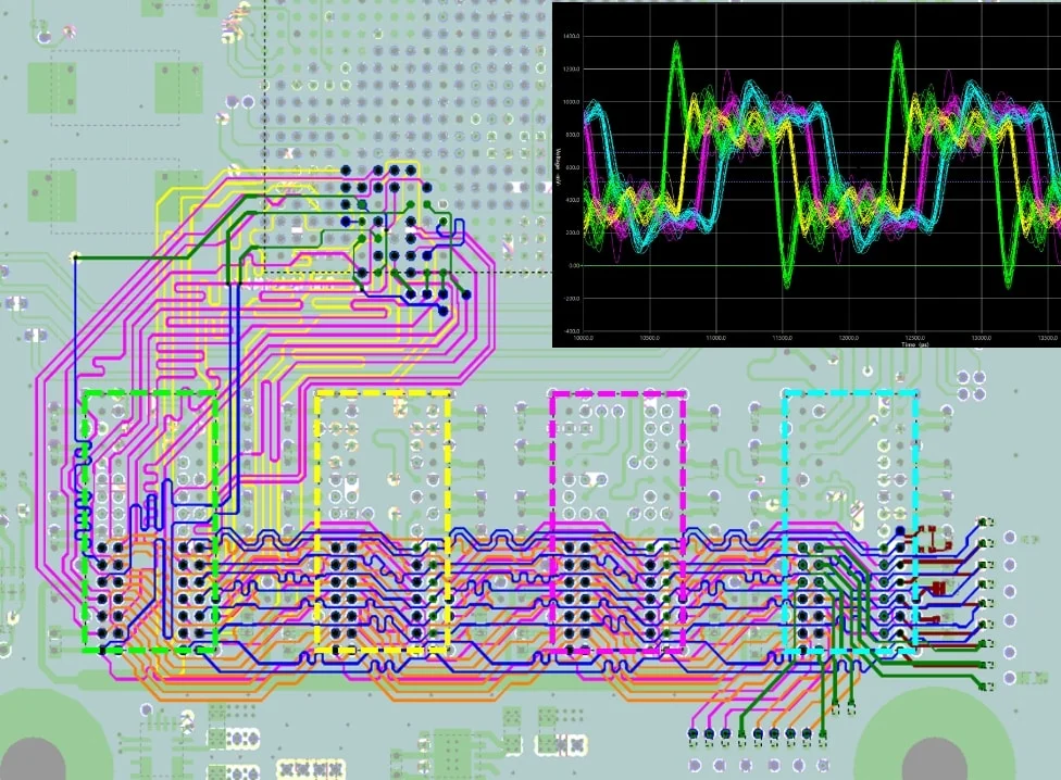
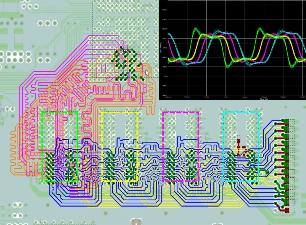
SI analysis
Pre-analysis
This is carried out before the board design. We examine the floor plan and construct a realistic design guide.
Layout of main components / Placement and values of passive components / Wiring layers, wiring lengths and connection methods / Device drive strength / Slew rate / Setting of interior termination
Post analysis
This is carried out using CAD data after the board design. If the specifications are deviated from, corrections are made to satisfy the requirements.
Signal quality verification / Delay and skew verification / Taking into account delay caused by vias and the difference in propagation speed between inner and outer layers
* Normally, handling is from post analysis, but pre-analysis can be handled if requested.
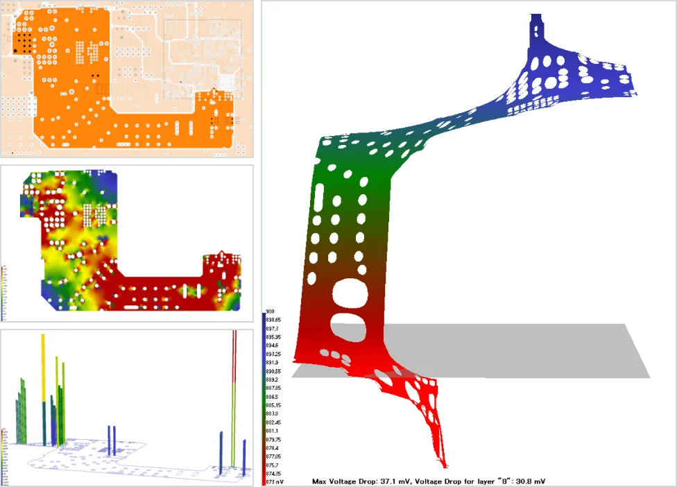
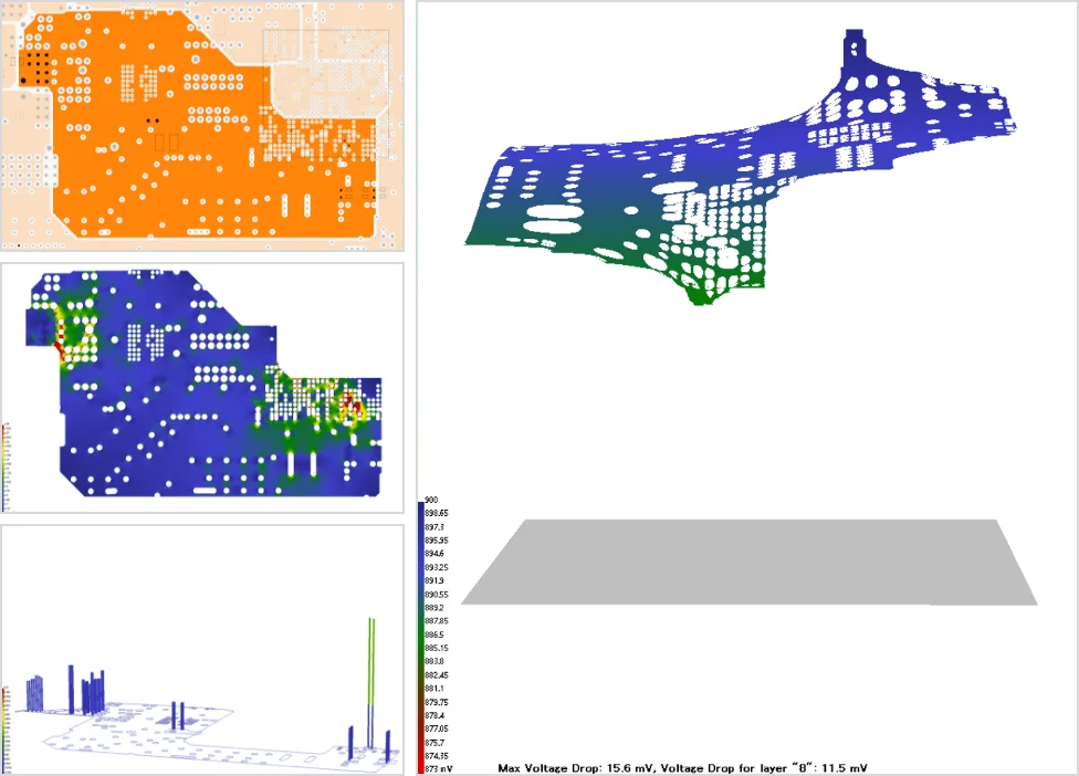
PI analysis
IR-Drop analysis (DC-Drop analysis)
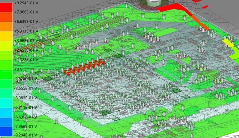
Voltage drop in the power plane (pattern) is analyzed.
The maximum current consumption is assumed, and verification is performed to ensure that it is within the operating voltage range of the device.
If the specifications are deviated from, corrections are made to satisfy the requirements.
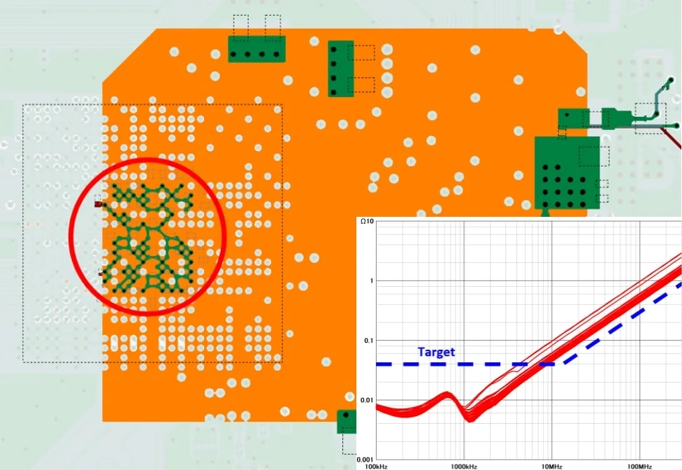
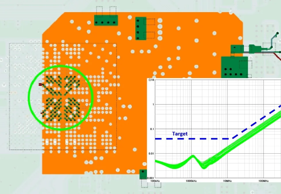
PDN Impedance analysis (decoupling analysis)
This is analysis with an aim of determining the effectiveness of bypass capacitors.
The input impedance seen from the power supply terminal of the device is analyzed, and the number, value, installation location, via design of the bypass capacitor, etc., are optimized.
Evaluation is performed in the frequency domain, and verification is performed using the target impedance as a guideline.
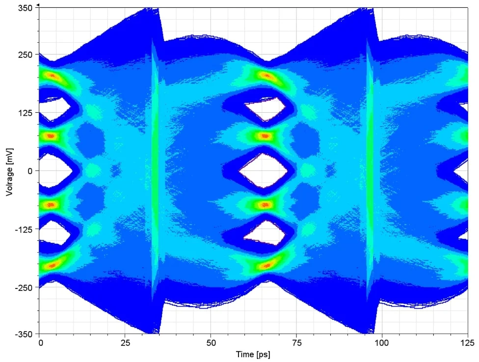
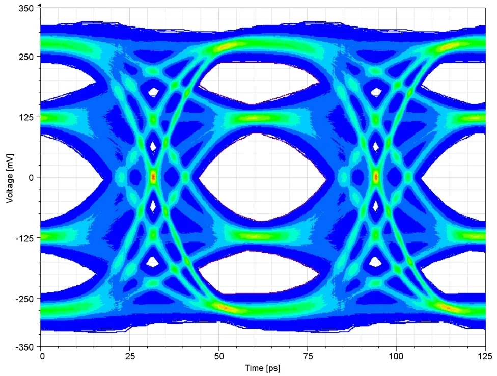
Electromagnetic field analysis
Highly precise analytical solutions are provided through the use of three-dimensional full-wave electromagnetic field analysis based on the finite element method, or a hybrid solver that incorporates the moment method.
Unlike SI analysis tools that handle transmission lines as equivalent circuits, the use of S-parameters in modeling takes frequency characteristics into account, enabling analysis that takes into account return paths, crosstalk, etc.
EMI suppression support
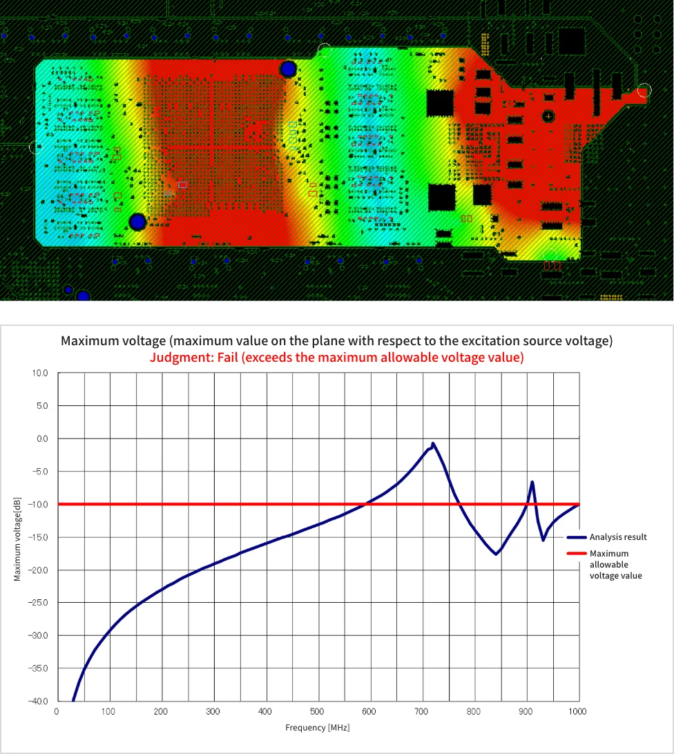
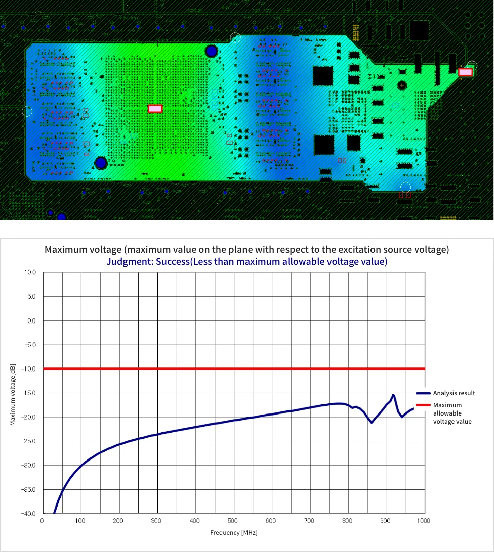
Plane resonance analysis
When resonance occurs between the power supply and GND planes in a multilayer board, EMI increases if the operating frequency in the circuit matches the resonance frequency.
Measures are taken to suppress these resonances.
EMI rule checking
The error screening function is used to identify the causes of EMI that have been made into rules, the necessary parts for countermeasures are extracted, and those are resolved at the PCB design stage.
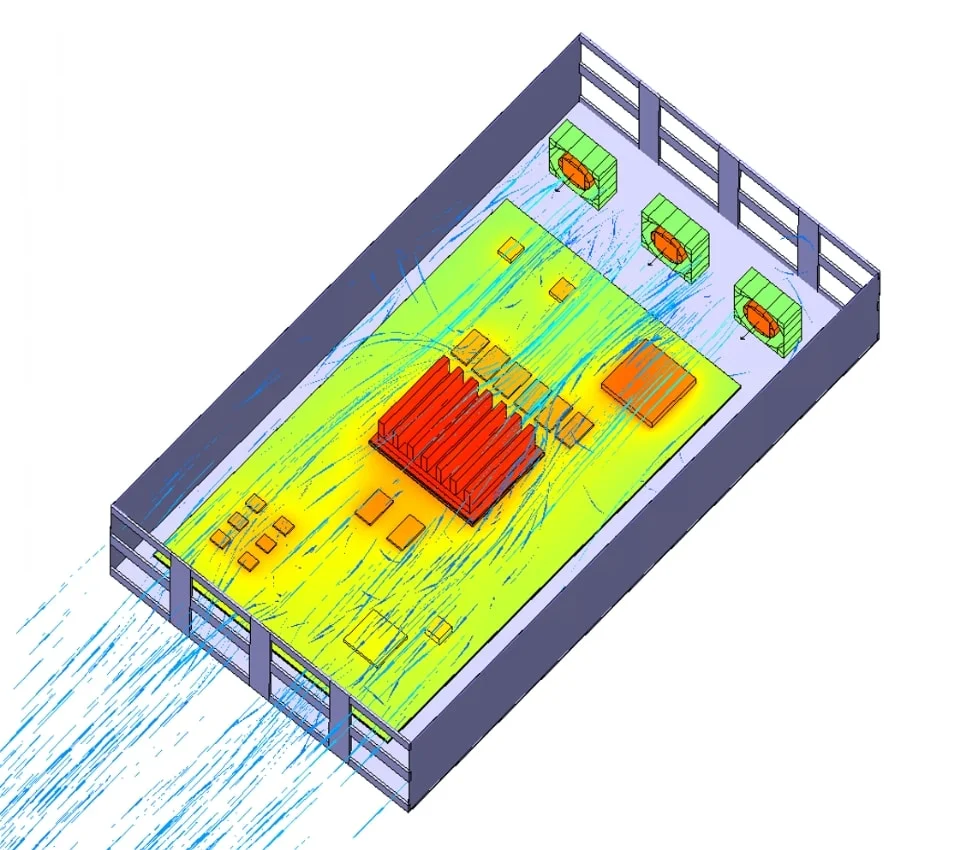
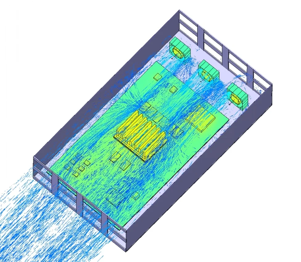
Thermal fluid analysis
The device temperature on the PCB and the amount of heat generated by the current flowing through the wiring pattern and via are analyzed.
In addition to thermal fluid analysis with the PCB installed in the housing, the cooling effect of the heat sink and fan can also be analyzed.
List of CAD software
| Category | Tool name | Manufacturer |
|---|---|---|
| SI | HyperLynx SI | SIEMENS |
| PI | HyperLynx PI | SIEMENS |
| Electromagnetic field | HFSS | Ansys |
| SIwave | Ansys | |
| HyperLynx Full-Wave Solver | SIEMENS | |
| EMI suppression | DEMITASNX | NEC |
| Thermal fluid | Simcenter Flotherm | SIEMENS |
| Simcenter Flotherm Pack | SIEMENS |
Noise consulting

In AI, 5G, IoT and other fields concerned with electronics, transferred signals are becoming faster and of higher frequency.
KYODEN offers assistance for resolving “noise” issues that cause concern to the engineers that work with such technologies.
Have you ever experienced the following kinds of problems regarding noise?
- Need to revise the
design because the
noise generated by
the existing PCB is
too large - Need to take care of
noise even with a
short development
schedule - Need to take
measures for the
housing and cables
and pass EMC
testing - Need to solve noise
issues from a third-
party perspective
KYODEN will support you in solving these
noise-related problems!
KYODEN’s strengths in noise consulting and the benefits for customers
-
For the cost and time of PCB
production plus a little extra,
design that takes care of noise
can be made.The cost of noise consulting alone will not
exceed the cost of PCB production. -
For development,
support at any stage is possible
(from component selection to EMC testing).It doesn’t matter whether you start
from the circuit
design stage
or after the device has been made. -
Even if
there are no designers familiar
with noise,
design and countermeasures can be done.iNARTE/KEC EMC Senior Design
Engineers provide strong support. -
Know-how (thought process + results)
as a
deliverable
is delivered.Deliverables include know-how
and numerical values
from the design
and countermeasure processes. -
In addition to PCBs, cables
and mechanical parts
are handled from a systems perspective. -
Measures taken based on
actual equipment
are possible
(moving your hands to get results).
Noise consulting by iNARTE EMC Engineers
(1) PCB noise-reducing design consulting
Proposals for noise countermeasures at the circuit diagram, component placement and wiring levels

(2) Noise countermeasures consulting
Countermeasure proposals examined on paper, countermeasures implemented on actual equipment and at the site, and on-site observation of testing

Circuit diagram input,
fair copy, BOM creation
Do you want to do your own circuit design, but don’t have the time or internal resources to input it into circuit diagram CAD?
KYODEN can also provide CAD input support.
In addition to converting hand-drawn circuit diagrams into CAD data, we can also merge reference boards with existing circuit diagrams, etc., regardless of whether they are new or revised, so please use us if you are having any problems.
- OrCAD Capture
- CR-8000 Design Gateway
- Deliverable
- - Circuit diagrams/netlists, BOMs, etc.

Parts library creation
We can also create parts libraries for use in PCB design.
- If you provide us with just a BOM, we will register and provide the components by the manufacturer’s model number in the BOM.
- We can provide libraries with layer structures that match your CAD environment.
- CAD software we can provide in: BoardDesigner, Allegro
- We have a parts library with over 190,000 parts, so we can provide them quickly.
- We can also create libraries that match your footprint creation standards.