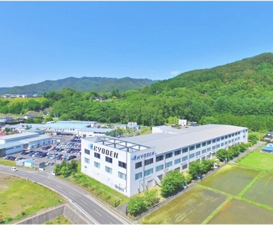
PCB MANUFACTURING

PCB MANUFACTURING

We achieve and complete built-in quality
in all manufacturing processes and stable supply by
constructing a mutually complementary structure
involving all of our manufacturing centers

From the short lead-time manufacture of a single board to the manufacture of PCB products in small and medium-sized lots, we
respond to the demands of customers with a diverse lineup of products centered around buildup PCBs and multilayer PCBs.

  • Diverse Product Lines

    • Single-sided/Double sided PTH PCBs

      We make PCBs that have circuit wiring installed on a single side or both sides of the epoxy resin
      surface. For Double sided PTH PCBs, the front and rear sides are connected via processing (hole drilling).
      KYODEN can deliver products in a minimum lead-time of 1 day.

      片面/両面基板
    • Multilayer PCBs

      In multilayer PCBs, copper circuit wiring is formed on the epoxy resin surface and multiple layers
      are adhered by heating.
      We can manufacture a wide variety of multilayer PCBs comprising between 4 and 54 layers,
      board thickness of 0.5mm-6.3mm, and various impedance control specifications.

      多層基板

      The table on the right shows
      specifications (reference) including
      board thickness and substrate
      materials corresponding to the
      number of layers. We can respond
      to customized requests,
      so please feel free to inquire.

      層数に応じた板厚、使用基材などの仕様

    • IVH PCBs

      Whereas conventional via processing penetrates the PCB,
      IVH is a method for manufacturing multilayer PCBs by using vias that connect only specific layers.
      Because the vias do not appear on the other layers,
      it is possible to increase the degree of circuit integration.

      IVH基板
    • High-density interconnect (“HDI”)

      In these PCBs for transmitting high-frequency signals,
      we use substrate materials that entail little high-frequency loss and low conductivity.
      Since the Tg, etc. differs from conventional FR-4 substrate material, special controls
      and equipment such as plasma washing machines, etc. are required in manufacturing.
      Ceramic (alumina) and Teflon materials are also used, among others.

      ビルドアップ基板
      HDI Any Layer PCBs

      Featuring a combination of laser technology, filled plating technology, etc.
      capable of ultrafine processing, these PCBs permit flexible connections across all layers.
      Because these PCBs enable a high degree of design flexibility and integration, they are ideally suited to increasing
      needs for smaller and thinner high-performance devices such as smartphones.

      エニーレイヤー基板
    • Microwave PCBs

      In these PCBs for transmitting high-frequency signals,
      we use substrate materials that entail little high-frequency loss and low conductivity.
      Since the Tg, etc. differs from conventional FR-4 substrate material,
      special controls and equipment such as plasma washing machines, etc. are required in manufacturing.
      Ceramic (alumina) and Teflon materials are also used, among others.

      高周波基板
      Mechanical back-drilling (minimal stub)

      Because through-holes along transmission lines cause signal quality to deteriorate in proportion
      to frequency, it is possible to reduce signal reflectivity and improve transmission line
      characteristics by removing through-hole excesses (stubs).

      バックドリル高多層基板
    • High-density PCBs

      We utilize the semi-additive method to manufacture ultrafine patterns.

      Peel strength of 10N/cm or higher

      By adopting UTC copper foil of 5μm as the primary coppering,
      stable peel strength is obtained irrespective of the type of substrate material,
      and abnormal precipitation of the gold plating caused by residual Pd is prevented.

      Adoption of via fill plating as electrolytic copper plating

      This makes it possible to suppress variations in plating thickness and respond to filled via requirements.

      Based on any layer stack structure and multistage buildup PCBs,
      we can respond to a wide variety of PCB needs ranging from
      double-sided boards to multilayer boards.

      微細パターン L/S=40/40

      Ultrafine pattern L/S=40/40

      5-2-5(AnyLayer) ビルドアップ配線板断面図

      5-2-5 (Any layer) Buildup PCB cross section

    • Heat-dissipating PCBs

      As electronic components acquire increasingly higher performance and become more and more
      compact, the amount of generated heat increases. From the standpoint of maintaining performance
      and extending the service life of electronic devices, it is necessary to adopt heat-dissipating circuitry
      that releases the heat generated in components from the space to the pattern.
      We propose solutions to these challenges in the shape of heat-dissipating measures.

      放熱基板
      Copper Paste Via Filling
      (heat conductivity 0.58~7.8W/mk)

      We can fill from small diameter vias of φ0.15. Moreover, our proprietary vacuum via filling technology can also adapt to the filling of bottomed vias.

      銅ペーストVIA穴埋め
      銅ペーストVIA穴埋め

      As electronic components acquire increasingly higher performance and become more and more compact, the amount of generated heat increases. From the
      standpoint of maintaining performance and extending the service life of electronic devices, it is necessary to adopt heat-dissipating circuitry that releases the heat
      generated in components from the space to the pattern. We propose solutions to these challenges in the shape of heat-dissipating measures.

    • Cupper Bump PCBs

      Available to form the bump(height 20μm~100μm) on the required position of circuit pattern

      バンプ基板
    • Flexible PCBs

      FPCs are PCBs in which the electric circuitry is arranged on a substrate material constructed by
      laminating a thin, soft, flexible, insulating base film (polyimide, etc.) with copper foil.
      Since these boards, including their wiring, are thin, flexible and can be freely bent, it is possible to
      make it possible to make smaller, lighter and thinner electronic devices and can be
      three-dimensionally fitted into very small gaps.

      フレキシブル基板

    In addition,
    we are advancing development of other special
    PCBs suited to a diverse range of technologies and uses.

    Go here for advanced technologies
  • A Solid Lineup of Manufacturing Centers

    • Tohoku Factory

      Product lines
      Double-sided and multilayer PCBs
      Production capacity
      28,000㎡
      Main products
      Amusement machines, automotive devices, AV-related devices, battery dev
      東北事業所
    • Nagano Factory

      Product lines
      Single layer-multilayer PCBs, High-density interconnect (“HDI”)
      Production capacity
      17,000㎡
      Main products
      Measurement devices, AV-related devices, telecommunications devices, electronic devices
      長野事業所
    • Osaka Factory

      Product lines
      High-density interconnect (“HDI”), Double-sided and multilayer PCBs, flexible PCBs
      Production capacity
      17,000㎡
      Main products
      Optical devices, high-frequency devices, sensors
      大阪事業所
    • Thailand Factory

      Product lines
      Double-sided and multilayer PCBs capacity
      Production capacity
      130,000㎡
      Main products
      Automotive devices, OA-related and office equipment, home electronics and AV-related devices
      タイ事業所

    Here for inquiries.

SUPPORT

If you would like help with PCBs,
leave it to KYODEN!

We can respond to all kinds of PCB needs and offer direct support from any stage.

基板製造のことならキョウデンにおまかせください。