Event


Converting customers’
ideas into reality

SCROLL


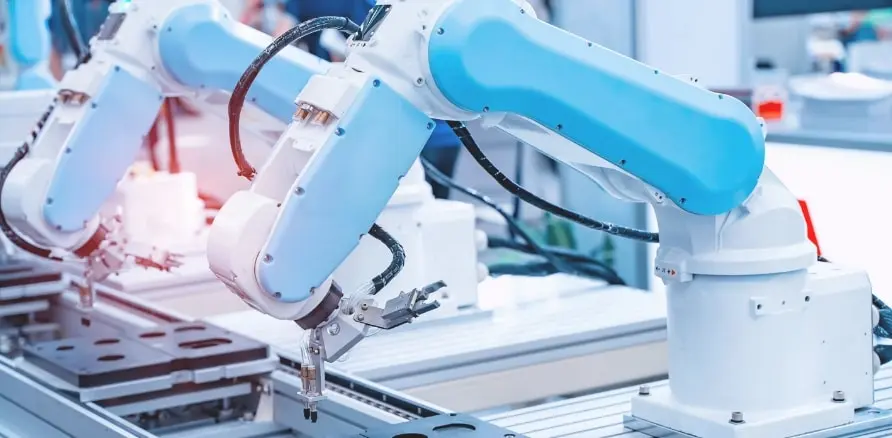
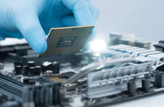
Solutions and Products
We respond to our customers’ product development issues by providing total
in-house integrated support
We also provide “total in-house production one-stop solutions” that no other company can offer by pursuing added value for products through our integrated support from the development stage even for custom components that make up products, such as PCBs, housings, and mechanical parts.


