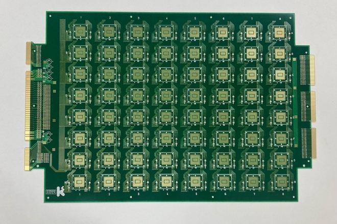
Semiconductor Testing PCB
Semiconductor Testing PCB are used for tests and inspections of semiconductor devices. They are mainly used in the semiconductor manufacturing industry and by electronic device manufacturers.
They contribute to improving the quality control and testing efficiency of semiconductor devices as they enable high-speed signal transmission and accurate signal processing.
Features
- This is an important type of PCB that is connected to a testing device by directly applying a probe to check for electrical issues in semiconductors.
- They are high aspect ratio PCBs that support high layer counts and small-diameter vias and for the miniaturization of circuits due to the increased number of pins and narrow pitch of semiconductor packages.
- They enable wiring of over 5,000 nets while ensuring high signal quality.
KYODEN’s Strengths
- We can handle from general materials to high Tg materials, and low dielectric materials.
- Plating processes for signal quality are also handled in-house. TH reliability is also high quality.
Development product: 70-layer through-hole PCBs + 2-stage and other build-up structures are also available
74 layers (2-70-2) t5.90
[Substrate used] Panasonic R-1566/R/1551
Main product uses
- Semiconductor testing equipment

