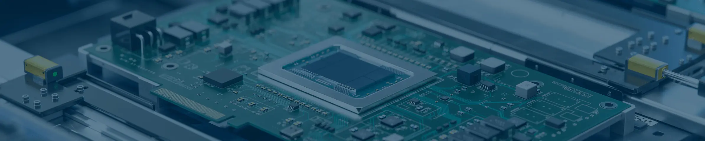
Cutting-edge technologies

Developing Technologies in
Response to New Market Needs
KYODEN’s PCBs continue to generate value in a truly diverse range of fields. From familiar everyday life to big industry,
various work sectors and areas where state-of-the-art technology is required.
We respond to our customers’ needs by leveraging advanced technology in PCBs for 5G communication,
high-multilayer PCBs, High-density interconnect (“HDI”), high-frequency,
high-density, high heat-dissipating, large-current PCBs, and more.
KYODEN’s PCBs Used
in a Wide Range of Fields
-

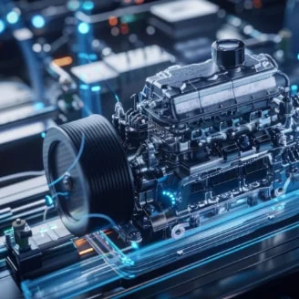
Industrial devices
- Robots, AGV and display devices
- Semiconductor manufacturing systems and 3D coordinate measuring machines
- Stepping motor controllers
- Power source controllers and inverters
-
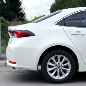
Automotive devices
- Millimetric wave sensors
Drive recorders - Multi-information displays
- ADAS-related devices
(automatic drive support systems) - Car navigation systems
ETC onboard units
- Millimetric wave sensors
-
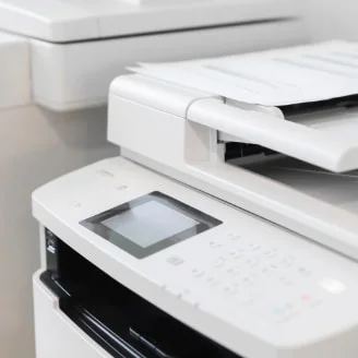
Office equipment and
precision devices- Copiers and multifunction machines
- POS systems
- Web conference systems
-
Sensors and module devices
- Wireless modules and power source modules
- Camera modules
- Power devices and LED
-

Amusement devices
- Home game consoles and casino devices
- Pachinko and pachinko-slot game units and interposed machines
-

Medical devices (CLASSⅠ-Ⅵ)
- Monitoring devices and physiological examination devices
- Artificial respirators, AED, MRI and CT examination systems
-
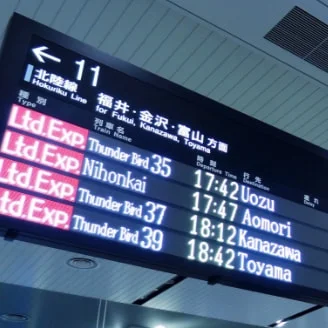
Infrastructure-related
- Railway control systems and bus and train destination electric display boards
- Disaster prevention and security devices and smart meters
-
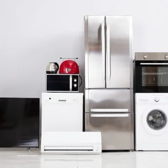
Household electrical appliances
(smart home appliances)- 4K/8K TVs and audio equipment
- Air conditioners, refrigerators, and healthcare equipment
-

Broadcasting equipment
- HDR editors and switchers
- 4K/8K video camera systems
-

Aerospace
- Private aviation-related devices
- Artificial satellite control systems
An Industry First! Contributions to Measures for Heat Dissipation
in PowerSemiconductor and High Heat-dissipating High-
frequency Components※Survey by KYODEN
Development of a high heat-dissipating, high-frequency PCB
based on the high-speed thick copper plating method
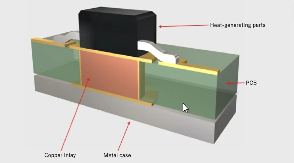
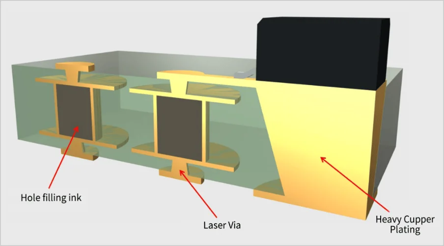
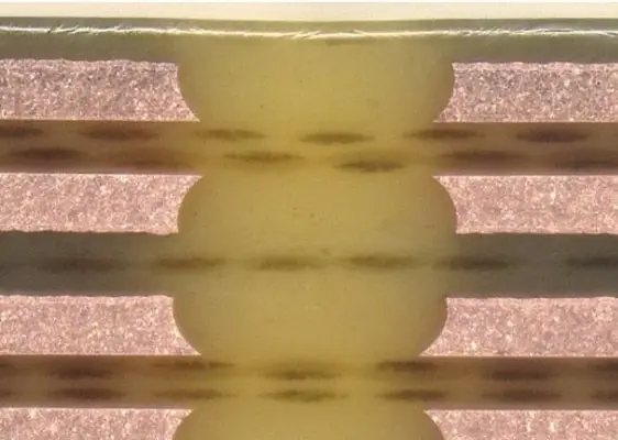
This PCB is structured with high-speed thick copper plating filled directly underneath heat-dissipating components,allowing the copper, which has high heat conductivity, to directly connect and dissipate heat below the circuit board.
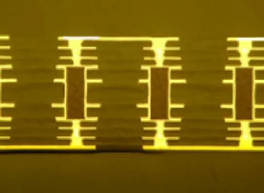
In conventional PCBs, copper inlays and copper coins (Figure 1) were embedded in the board for the purpose of dissipating heat. However, issues were presented in terms of mass productibility, PCB reliability and compatibility with thin boards.
In response to these challenges, we have developed high-speed thick copper plating technology and succeeded in making high heat-dissipating, high-frequency PCBs (Figure 2).
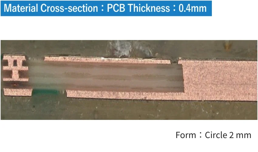
Since this product uses thick copper plating, shape and size can be freely set, making it possible to assemble buildup layers that were previously difficult to achieve with aluminum boards and copper-base boards (Figure 3).
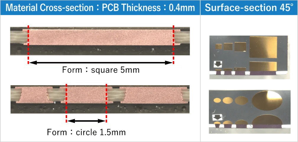
Moreover, this technology can also be applied to PCBs for thin plate components of 0.4mm or less, which cannot be handled with a copper inlay, thereby contributing to heat dissipation in high heat-radiating components. It has thus become possible to respond to needs for high frequency and high heat-dissipation in power amp and power
semiconductor components used in 5G/6G base stations.
Reliability assurance
Also, in PCB reliability verification,
this technology clears
our in-house standard.
- Hot oil test: 260℃/10 seconds→20℃/20 seconds, 100 cycles
- Cold impact test: -40℃ (30 minutes) ⇔125℃ (30 minutes), 500 cycles
- Solder heat-resistance test: 20 second floating in a solder bath of 260℃, 5 cycles
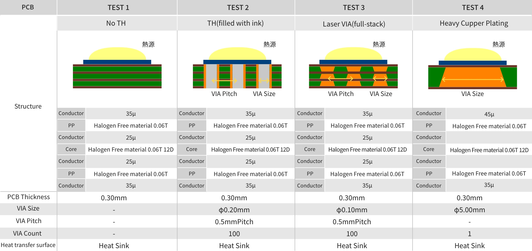
Moreover, the superior characteristics of the thick copper plating structure have been verified in heat dissipation
simulations and verification experiments assuming various PCB structures (Figure 5 and Figure 6).
Models for examining each board structure
Simulation Conditions
※Chip heat generation: 10W (5W setting
under Condition 1 only)
※PCB (bottom face): Constant 25℃
cooling, PCB (top face): Natural cooling
PCB From:50mm×50mm
Heating Element:5mm×5mm
Pat Size:6mm×6mm
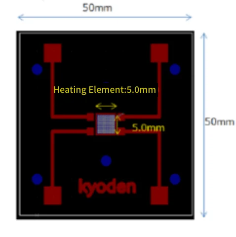
Simulation condition
※chip heat value:10W(test 15w)
※PCB upper side: natural cooling , PCB below side: constant cooling 25°C
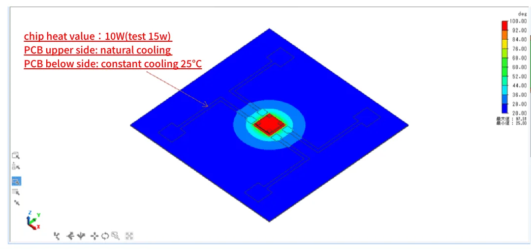

Heat Dissipation Effect (transient analysis)

Based on the results of simulation, we confirmed the heat dissipation effect (effect on heat
dissipation speed) due to applying thick copper plating vias to a PCB directly under a chip.
Advanced Technological Capabilities Responding
to Diverse Needs
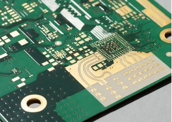
By leveraging cutting-edge, advanced technological capabilities, we provide products that respond to the needs of our customers, ranging from general through-hole-type PCBs to high-density wiring PCBs for use in smartphones, etc., high-frequency PCBs for supporting advances in IoT and mobility, and heat-dissipating and flexible PCBs that can withstand harsh environments.
-
General through-hole PCBs
Single-sided/Double sided/multilayer PTH PCBs -
High-density circuit boards
High-density interconnect (“HDI”) 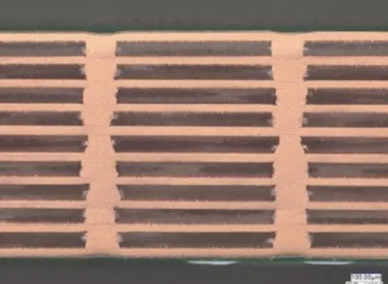
HDI Any Layer PCBs -
High heat-dissipating and thick copper circuit boards
Heavy Copper PCB 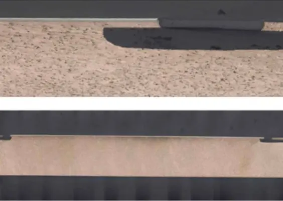
Metal base heat-dissipating PCBs 
High heat-dissipating PCBs(high-
speed heavy copper plating) -
High-speed communication and high-frequency circuit boards
High Frequency Millimeter-wave PCB 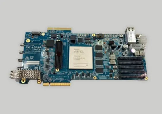
High-speed transmission PCBs 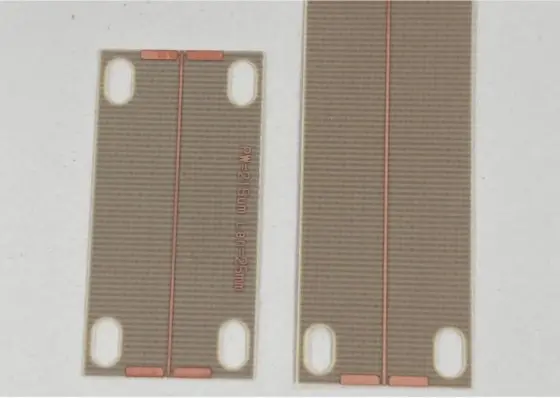
RF module PCBs -
Multilayer and high aspect ratio circuit boards
Semiconductor Testing PCB 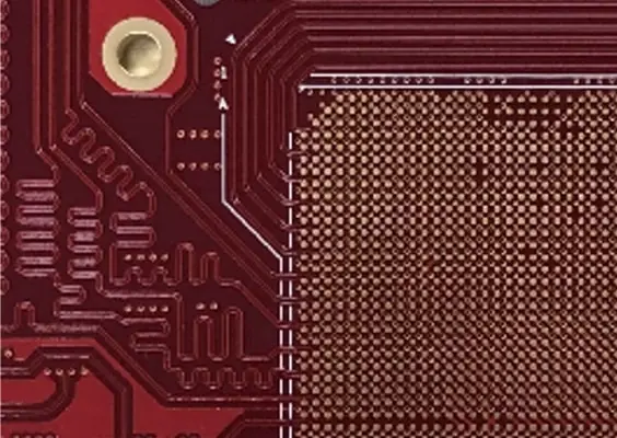
Semiconductor Testing PCB -
Flexible circuit boards
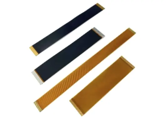
Flexible PCBs
Click here for details on each product