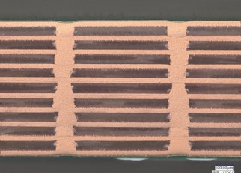
HDI Any Layer PCBs
This is a type of High-density interconnect (“HDI”), and it is manufactured using laser vias and filled plating technology for all layers. These PCBs allow free wiring on all layers.
It has a high degree of design freedom, and can be made denser, smaller, and thinner, making it ideal for meeting needs for making high-performance device equipment such as PCBs for cameras and the like thinner and more compact.
Features
- The full stack structure (AnyLayer) with all layers having filled vias allows for flexible connections.
- The degree of freedom in artwork design is high, making it compatible with small products and irregular shapes.
- It is suitable for making PCBs thinner and more compact, and compatible with miniaturization of the size of mounted components.
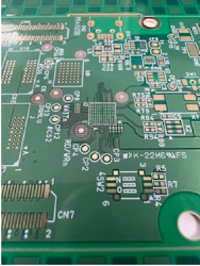
Main product uses
- Devices that use narrow-pitch BGAs, etc.
- Security camera equipment
- Main PCBs for communication devices, etc.

