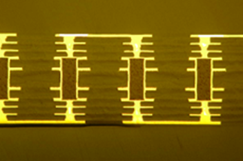
High-density interconnect (“HDI”)
This is a multilayered printed circuit board in which conductors are stacked one layer at a time on top of the core layer. It is a PCB with multilayer structure that is manufactured by repeatedly drilling holes, wiring, and forming vias.
Using laser via technology, which can form small holes, and filled plating technology, it is possible to construct a variety of layer configurations in the buildup layer and core layer. Therefore, it has a higher degree of design freedom than multilayer through-hole PCBs, and is suitable for making products smaller and thinner.
Features
- It is possible to make the PCB more compact compared to through-hole PCBs.
- In the case of through-hole via-less, the conductor thickness can be reduced, so there are benefits in terms of making the surface flat when surface mounting.
- Because the interlayer thickness is thin, there is little transmission loss, making it ideal for high-speed transmission applications.
- Because the build layer can be connected to the interlayer for each layer, it is possible to route the wiring on the upper part (layer), making it possible to achieve high density.
KYODEN’s Strengths
- The degree of freedom for wiring is improved by using a full stack structure with filled vias for the buildup layer.
- We can propose substrates with the characteristics you want, thanks to our inventory of substrates and extensive prototyping experience.
- We can make PCBs ultra-thin fine using ultra-thin materials. (Smallest possible board thickness: 0.40mm (1-2-1))
- 1-2-1 (four-layer High-density interconnect (“HDI”)) are delivered in as short as 2 days.
- The latest laser processing machines are introduced along with in-house via-fill plating lines. This achieves stable quality.
- We have two High-density interconnect (“HDI”) manufacturing plants. This gives reassurance from a BCP perspective as well.
Main product uses
- Mobile information and communication devices such as smartphones, tablets, and notebook PCs


